Navigation

    M5Stack Community

    • Register
    • Login
    • Search
    • Categories
    • Recent
    • Tags
    • Popular
    • Users
    • Groups
    • Search
    1. Home
    2. JiKuch
    3. Posts
    J
    • Continue chat with JiKuch
    • Start new chat with JiKuch
    • Flag Profile
    • Profile
    • Following
    • Followers
    • Blocks
    • Topics
    • Posts
    • Best
    • Groups

    Posts made by JiKuch

    • RE: M5 POWER BANK with IP5108

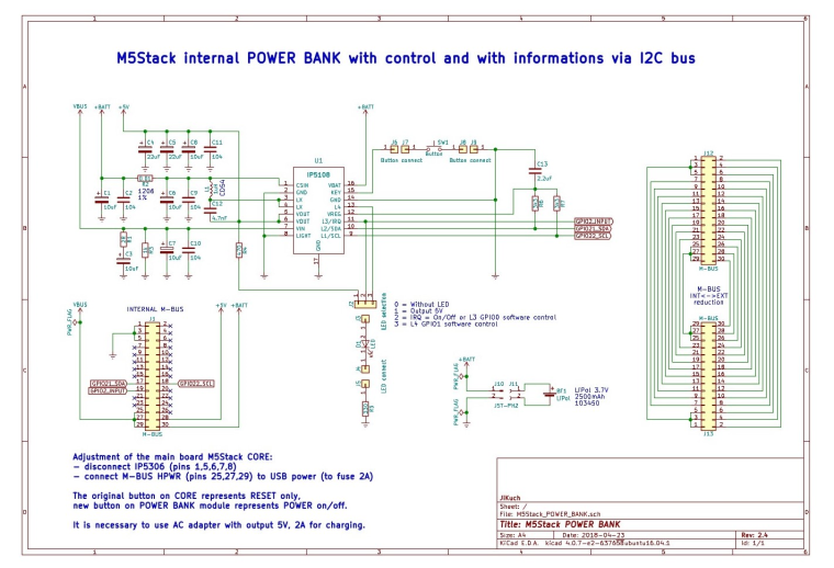
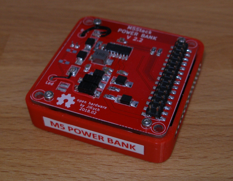
      IP5108 I2C description:

      7-bit slave address IP5108 is 0x75 (byte with write bit = 0xEA; byte with read bit = 0xEB)
      400 Kbps speed of I2C supported
      1 byte data = 8-bit data (bits from 7 to 0)

      WRITE Arduino example:
      Wire.beginTransmission(0x75);
      Wire.write(register_address_byte);
      Wire.write(data_byte);
      Wire.endTransmission();

      READ Arduino example:
      Wire.beginTransmission(0x75);
      Wire.write(register_address_byte);
      Wire.endTransmission();
      Wire.requestFrom(0x75,1);
      data_byte = Wire.read();

      REGISTERS:

      1. Enable / disable functions:
      SYS_CTL0 = 0x01:

      • bit 4 (read/write): 0 = disbale / 1 = enable (1 = after reset) detection ??? (I do not understand.)
      • bit 3 (read/write): 0 = disbale / 1 = enable (1 = after reset) light
      • bit 2 (read/write): 0 = disbale / 1 = enable (1 = after reset) booster
      • bit 1 (read/write): 0 = disable / 1 = enable (1 = after reset) charger

      SYS_CTL1 = 0x02:

      • bit 1 (read/write): 0 = disable / 1 = enable (1 = after reset) auto-standby
      • bit 0 (read/write): 0 = disable / 1 = enable (1 = after reset) auto ??? (I do not understand.)

      SYS_CTL3 = 0x03:

      • bit 5 (read/write): 0 = disable / 1 = enable (1 = after reset) off by button

      2. General setup features:
      SYS_CTL2 = 0x0C:

      • bits 7-3 (read/write): (01010 = after reset) auto-standby current limit as multiple 12 mA

      SYS_CTL4 = 0x04:

      • bits 7-6 (read/write): (10 = after reset) time for auto-standby: 00=8s, 01=16s, 10=32s, 11=64s

      SYS_CTL3 = 0x03:

      • bits 7-6 (read/write): (01 = after reset) time for recognition button press: 00=1s, 01=2s, 10=3s, 11=4s

      SYS_CTL5 = 0x07:

      • bit 1 (read/write): (0 = after reset) control of light by button: 0=press, 1=double click
      • bit 0 (read/write): (0 = after reset) off by button: 0=double click, 1=press

      3. Charging setup features:
      CHARGER_CTL1 = 0x22:

      • bits 3-2 (read/write): (01 = after reset) VOUT undervoltage limit during chargig: 00=4.53V, 01=4.63V, 10=4.73V, 11=4.83V

      CHARGER_CTL2 = 0x24:

      • bits 6-5 (read/write): (00 = after reset) battery type = charging voltage: 00=4.2V, 01=4.3V, 10=4.35V
      • bits 2-1 (read/write): (10 = after reset) overcharging of charging: 00=0mV, 01=14mV, 10=28mV, 11=42mV

      CHG_DIG_CTL4 = 0x25:

      • bits 4-0 (read/write): (10110 = after reset) charging current setting [A]:
        b0 x 0.1 + b1 x 0.2 + b2 x 0.4 + b3 x 0.6 + b4 x 1.4

      4. Charging information:
      Reg_READ0a = 0x70:

      • bit 3 (read only): charging status: 0 = not charging, 1 = charging

      Ref_READ0b = 0x71:

      • bits 7-5 (read only): detailed charging status:
        000 = inactivity
        001 = charging
        010 = constant current charging
        011 = charging with constant voltage
        100 = ??? (missing description in original document)
        101 = end of charging (maintenance current)
      • bit 3 (read only): signal of end of charging (=1)

      5. PIN assignment & control:
      MFP_CTL0 = 0x51:

      • bits 5-4 (read/write): (00 = after reset) pin LIGHT assignement: 00=WLED, 01=GPIO2, 10=VREF
      • bits 3-2 (read/write): (00 = after reset) pin L4 assignement: 00=L4, 01=GPIO1
      • bits 1-0 (read/write): (00 = after reset) pin L3 assignement: 00=L3, 01=GPIO0

      GPIO_CTL2a = 0x53:

      • bits 2-0 (read/write): (000 = after reset) GPIO[2:0] input enable

      GPIO_CTL2b = 0x54:

      • bits 2-0 (read/write): (000 = after reset) GPIO[2:0] output enable

      GPIO_CTL3 = 0x55:

      • bits 2-0 (read/write): (000 = after reset) GPIO[2:0] data

      6. Measurement:
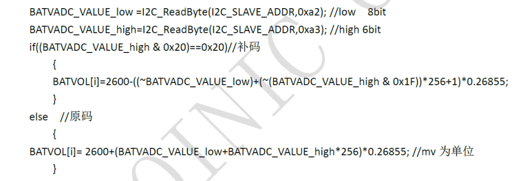
      BATVADC_DAT0 = 0xA2:

      • pins 7-0 (read only): LOW 8 bits (byte) of BATVADC

      BATVADC_DAT1 = 0xA3:

      • pins 5-0 (read only): HIGH 6 bits of BATVADC

      Calculation according to the original document:
      0_1535826835366_BATVADC.png

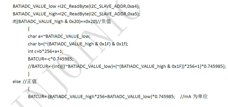
      BATIADC_DAT0 = 0xA4:

      • pins 7-0 (read only): LOW 8 bits (byte) of BATIADC

      BATIADC_DAT1 = 0xA5:

      • pins 5-0 (read only): HIGH 6 bits of BATIADC

      Calculation according to the original document:
      0_1535825484785_BATIADC.png

      BATOCV_DAT0 = 0xA8:

      • pins 7-0 (read only): LOW 8 bits (byte) of BATOCV

      BATOCV_DAT1 = 0xA9:

      • pins 5-0 (read only): HIGH 6 bits of BATOCV

      Calculation according to the original document:
      0_1535825504468_BATOCVADC.png

      This is true: BATOCV = BATVACD + BATIADC * battery_internal_resistnace

      7. WLED status:
      Reg_READ1 = 0x72:

      • bit 7 (read only): 0 = WLED is off, 1 = WLED is on

      8. Light / heavy load:
      Reg_READ1 = 0x72:

      • bit 6 (read only): 0 = heavy load over 75 mA, 1 = light load less 75 mA

      9. Button control:
      Reg_READ2 = 0x77:

      • bit 3 (read; write 1 = reset) flag button double clicked (=1)
      • bit 1 (read; write 1 = reset) flag button pressed (=1)
      • bit 0 (read; write 1 = reset) flag button clicked (=1)

      That is all.

      posted in PROJECTS
      J
      JiKuch
    • RE: IP5306 automatic standby

      Who is interested in the IP5108 solution, so look at the implementation in the section PROJECTS:
      M5 Power Bank with IP5108

      posted in FAQS
      J
      JiKuch
    • M5 POWER BANK with IP5108

      Under this link IP3506 AUTOMATIC STANDBY was discussed the M5 Power Bank module.
      Here is the inspiration from the realization of this module:

      1. Schema
        0_1531661662908_M5Stack_Power_Bank_V24.png

      2. BOM
        0_1531661684833_M5_Power_Bank_BOM.png

      3. PCB for hand soldering
        0_1531661724055_M5_Power_Bank_PCB.png

      4. Case - 3D printed
        0_1531661759214_M5_Power_Bank_Case.png

      5. Final functional module
        0_1531661809513_M5_Power_Bank_Module.png

      M5 Power Bank with IP5108 fully replaces M5 BOTTOM:

      • The module also contains a magnet (big one)
      • External M-bus (fully) is on the right side (female 2x15)
      • LED indicator and On/Off button is on the left side
      • LED functionality can be selected (5V, On/Off=IRQ, GPIO00 or GPIO01 software control)
      • On/Off button functionality can also be programmed thru IP5108 registers

      WARNING:
      The module is designed to be connected directly to the M5 CORE because the components enter the space of M5 CORE!

      posted in PROJECTS
      J
      JiKuch
    • RE: IP5306 automatic standby

      Hi JimiT.

      Unfortunately, I did not get IP5306. This version 1.0 of M5Stack POWER BANK will not be implemented. I'm creating version 2.0 with IP5108, which is available:

      0_1516457944820_b7aa6a0d-f4eb-4a7c-9ad2-a962f0887a4c-image.png

      IP53108 can be purchased here, for example:
      https://www.aliexpress.com/store/1816136?spm=2114.10010108.100005.2.7cb76625aejUQV
      LiPol 103450 with capacity 2.500mAh here, for example:
      https://www.aliexpress.com/store/715509?spm=2114.10010108.100005.2.536685a84W2wpg

      If I create M5Stack POWER BANK, I will continue in the section projects.
      This FAQS contains problem with the IP5306 and it is a pity that the M5Stack team does not respond and does not inform: the last delivery, which I received, contained the M5Stack in black with IP5306_CK, which does not have an automatic standby! Hurray!

      posted in FAQS
      J
      JiKuch
    • RE: IP5306 automatic standby

      To solve the problem with IP5306, I decided to implement the BATTERY MODULE with IP5306_I2C as follows:
      0_1515402962456_97994060-2969-49dc-ad9c-7b3887d95a17-image.png
      The implementation will be as soon as I can buy IP5306_I2C.
      I welcome any comments and suggestions.

      posted in FAQS
      J
      JiKuch
    • RE: IP5306 automatic standby

      I get the answer from the manufacturer of IP5306 (Injoinic Tech):

      1. You can use IP5306_CK,this version always output 5V.
      2. I2C function only apply to IP5306_I2C custom design. you can order samples use the name: IP5306_I2C.
      3. Accessory is the I2C register document of IP5306, you can use IP5306_I2C, then modify IP5306's register(reg0x00[1]=1) to make IP5306 always output 5V.

      英集芯科技 Injoinic Tech
      陈 卫
      公司网址:http://www.injoinic.com
      邮箱:chenwei086@injoinic.com
      QQ : 248371522
      地址:广东省珠海市唐家湾高新区南方软件园A1栋8楼

      posted in FAQS
      J
      JiKuch
    • IP5306 automatic standby

      I was thinkig to use M5Stack for battery powered solution with low consuption. I encountered the problem with IP5306: At low power consuption below 45 mA (it's enough to turn off the LCD LED and turn ESP32 in modem-sleep) the VOUT = VCC_5V of ISP5306 is disconnected after 32 seconds and therefore ESP32 is not powered. Do you have any solution how to teach the IP5306 do not switch to standby automaticaly? It's a shame that the IP5306_I2C has not been used (controlled over I2C).

      posted in FAQS
      J
      JiKuch
    • GROVE I2C 5V or 3.3V?

      M5Stack is the perfect platform for the professional design of own solutions.
      I have received first CORE development kit wit ESP32 and tested Arduino examples.
      I have not encountered an unsolvable problem.

      However, I would like to ask you to clarify the following:

      1. What does HPWR represent in M-BUS? What is it good for?

      2. I did not find the GROVE I2C connection in the schematic. Since it contains 5V power level, does it mean that both SCL and SDA have a 5V pullup (with level conversion to ESP32)? Or is SDA and SCL connected directly to GPIO21 and GPIO22 without level conversion and need to keep up to 3.3V for GROVE SCL and SDA?

      Thanks in advance for your answer.

      posted in FAQS
      J
      JiKuch