COMMU design/scematic error
-
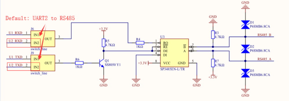
The RS485 interface design for the COMMU appears to be wrong. As shown, the transmit data (TXD) is used to enable/disable the driver on the DE/RE pins, while the driver data input, DI is permanently strapped low.
This means that sending data will drive a 'one' or float the line, but never drive a 'zero'.
The correct implementation should be TXD connected to the DI pin and a third signal used to control the DE/RE pins.
Since there is no third signal available, this design is fundamentally broken and won't interoperate with my existing systems.
V
